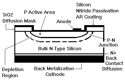
Silicon photodiodes are constructed from single crystal
silicon wafers . The purity of silicon is directly related to its resistivity,
with higher resistivity indicating higher purity silicon. A cross section of a typical silicon
photodiode is shown in the figure. N type silicon is the starting material. A
thin "p" layer is formed on the front surface of the device by
thermal diffusion or ion implantation of the appropriate doping material
(usually boron). The interface between the "p" layer and the
"n" silicon is known as a pn junction. Small metal contacts are
applied to the front surface of the device and the entire back is coated with a
contact metal. The back contact is the cathode, the front contact is the anode.
The active area is coated with either silicon nitride, silicon monoxide or
silicon dioxide for protection and to serve as an anti-reflection coating. The
thickness of this coating is optimized for particular irradiation wavelengths.
As an example, a Centro Vision Series 5-T photodiode has a coating which
enhances its response to the blue part of the spectrum.
Photodiode junctions are unusual because the top
"p" layer is very thin. The thickness of this layer is determined by
the wavelength of radiation to be detected. Near the pn junction the silicon
becomes depleted of electrical charges. This is known as the "depletion
region". The depth of the depletion region can be varied by applying a
reverse bias voltage across the junction. When the depletion region reaches the
back of the diode the photodiode is said to be "fully depleted". The
depletion region is important to photodiode performance since most of the
sensitivity to radiation originates there. The capacitance of the pn junction
depends on the thickness of this variable depletion region. Increasing the bias
voltage increases the depth of this region and lowers capacitance until the
fully depleted condition is achieved. Junction capacitance is also a function
of the resistivity of silicon used and active area size.

Due to concentration gradient, the diffusion of electrons
from the N- type region to the P-type region and the diffusion of holes from
the P- type region to the N-type region, develops a built-in voltage across
the junction. The inter-diffusion of electrons and holes
between the N and P regions across the junction results in a region with no
free carri- ers. This is the depletion region. The built-in voltage across the
deple- tion region results in an electric field with maximum at the junction
and no field outside of the depletion region. Any applied reverse bias adds to
the built in voltage and results in a wider depletion region.The electron-hole
pairs generated by light are swept away by drift inthe depletion region and are
collected by diffusion from the undepleted region. The current generated is
proportional to the incident light or radiation power. The light is absorbed
exponentially with distance and is proportional to the absorption coefficient.
The absorption coefficient is very high for shorter wavelengths in the UV
region and is small for longer wavelengths . Hence, short wavelength photons
such as UV, are absorbed in a thin top surface layer while silicon becomes transparent
to light wavelengths longer than 1200 nm. Moreover, photons with energies
smaller than the band gap are not absorbed at all. The boundaries of the
depletion region act as the plates of a parallel plate capacitor. The junction
capacitance is directly proportional to the diffused area and inversely
proportional to the width of the depletion region. In addition, higher
resistivity substrates have lower junction capacitance. In photoconductive mode
(reverse biased), however, the drift current becomes the dominant current (dark
current) and varies directly with temperature.
As time constant is directly proportional to capacitance, therefore,
lower the capacitance, lesser will br time constant and hence lesser will be
response time.