Dielectric Heating


A dielectric is an electrical insulator that can be polarized by an applied electric field. When a dielectric is placed in an electric field, electric charges do not flow through the material as they do in a conductor, but only slightly shift from their average equilibrium positions causing dielectric polarization. Because of dielectric polarization, positive charges are displaced toward the field and negative charges shift in the opposite direction. This creates an internal electric field which reduces the overall field within the dielectric itself. If a dielectric is composed of weakly bonded molecules, those molecules not only become polarized, but also reorient so that their symmetry axis aligns to the field.
The most obvious advantage to using such a dielectric material is that it prevents the conducting plates on which the charges are stored from coming into direct electrical contact. More significant, however, a high permittivity allows a greater charge to be stored at a given voltage.
Dielectric heating, also known as electronic heating, RF heating, high-frequency heating and diathermy, is the process in which a high-frequency alternating electric field, or radio wave or microwave electromagnetic radiation heats a dielectric material. At higher frequencies, this heating is caused by molecular dipole rotation within the dielectric.RF dielectric heating at intermediate frequencies, due to its greater penetration over microwave heating, shows greater promise than microwave systems as a method of very rapidly heating and uniformly preparing certain food items, and also killing parasites and pests in certain harvested crops.
Molecular rotation occurs in materials containing polar molecules having an electrical dipole moment, with the consequence that they will align themselves in an electromagnetic field. If the field is oscillating, as it is in an electromagnetic wave or in a rapidly-oscillating electric field, these molecules rotate to continuously align with it. This is called dipole rotation. As the field alternates, the molecules reverse direction. Rotating molecules push, pull, and collide with other molecules (through electrical forces), distributing the energy to adjacent molecules and atoms in the material. Once distributed, this energy appears as heat.
Temperature is the average kinetic energy (energy of motion) of the atoms or molecules in a material, so agitating the molecules in this way increases the temperature of the material. Thus, dipole rotation is a mechanism by which energy in the form of electromagnetic radiation can raise the temperature of an object. Dipole rotation is the mechanism normally referred to as dielectric heating, and is most widely observable in the microwave oven where it operates most efficiently on liquid water, and much less so on fats and sugars. This is because fats and sugar molecules are far less polar  than water molecules, and thus less affected by the forces generated by the alternating electromagnetic fields.

Flyback Transformers


Flyback transformers, popularly known as the Line Output Transformers, is a special mechanism of converting the energy supply, both voltage and current, into electronic circuits. Although it is termed as a transformer, it works against the typical functions of a conventional transformer, and is exploited more as energy storage equipment. When the primary switch is on, the energy is stored on ferrite core that has the air gap in it. However, when the primary switch is off, the energy is not stored but transferred to the outputs. The current will flow either in the primary winding, or the secondary one, but not both at the same time. Thus, a flyback transformer is often misguided to be an inductor having the secondary windings.


The primary  winding of the flyback transformer  is wound first around a ferrite rod, and then the secondary is wound around the primary. This arrangement minimizes the leakage inductance of the primary. A ferrite frame is wrapped around the primary/secondary assembly, closing the magnetic field lines. Between the rod and the frame is an air gap, which increases the reluctance. The secondary is wound layer by layer with enameled wire.
The primary winding of the flyback transformer is driven by a switch from a DC supply (usually a transistor). During the switch on time, there wont be any power conversion from primary to secondary side, since secondary side diode will be reverse biased, hence energy is stored in the inductor itself. In order to store the energy in magnetic field we use airgap in the inductor. but if it is too large, leakage inductance problem will occur. So provide airgap with minmum as per calculation obtained. 
When switch is off, the stored energy in the inductor(primary) will be transfered to the secondary. Through diode the capacitor will get charged. and this stored energy in the capacitor will be discharged when switch is in ON. The cycle then can be repeated. If the secondary current is allowed to discharge completely to zero (no energy stored in the core) then it is said that the transformer works in discontinuous mode. When some energy is always stored in the core then this is continuous mode.
Once the voltage reaches such level as to allow the secondary current to flow, then the current in the secondary winding begins to flow in a form of a descending ramp signal.
The current does not flow simultaneously in primary and secondary (output) windings. Because of this the flyback transformer is really a loosely coupled inductor rather than classical transformer, in which currents do flow simultaneously in all magnetically coupled windings.

Cuk Converter


The Cuk converter is a step-down/step-up converter based on a switching boost-buck topology. Essentially, the converter is composed of two sections, an input stage and an output stage.
The input voltage vg is fed into the circuit via inductor L1. When transistor Q1 is on, current i1 builds the
magnetic  field of the inductor in the input stage. The diode CR1 is reverse biased, and energy dissipates
from the storage elements in the output stage. When Q1 turns off, inductor L1 tries to maintain the current flowing through it by reversing polarity and sourcing current as its magnetic field collapses. It thus provides energy to the output stage of the circuit via capacitor C1. R1 and R2 are parasitic or stray resistances of inductor.


The inductor currents are the input and output currents, therefore, if the principle of conservation of energy is applied:


where Ds is the duty cycle of the switch :


The voltage ratio of a Cuk converter is the same as that of a buck-boost converter, but its main advantage over other converters is that the input and output inductors result in a filtered current on both sides of the converter, while buck, boost, and buck-boost converters have a pulsating current that occurs on at least one side of the circuit i.e either on input side or output side.
This pulsation will increase the ripple in the circuit and due to this ripple , the efficiency of battery gets lowered. To ensure good efficiency ripple should be reduced.
By controlling the duty cycle of the switch , the output voltage vo  can be controlled and can be higher or lower than the input voltage vg. By using a controller to vary the duty cycle during operation, the circuit can also be made to reject disturbances ,as second part of circuit consists of parallel resonance circuit and it work as a tank circuit for specific frequency (resonant frequency) , and during resonance current will not be allowed to enter in the circuit.

Series Resonance


In a series RLC circuit there becomes a frequency point were the inductive reactance of the inductor becomes equal in value to the capacitive reactance of the capacitor. In other words, XL = XC. The point at which this occurs is called the Resonant Frequency point, ( Æ’r ) and as we are analysing a series RLC circuit this resonance frequency produces a Series Resonance circuit.

As the frequency approaches infinity the inductors reactance would also increase towards infinity with the circuit element acting like an open circuit. However, as the frequency approaches zero or DC, the inductors reactance would decrease to zero, causing the opposite effect acting like a short circuit. This means then that inductive reactance is "Proportional" to frequency and is small at low frequencies and high at higher frequencies.

The major difference between series and parallel resonance is that due to the formation of Tank Circuit , large amount of circulating current exists and it will be exactly oppositely following series resonance current curve.   

As the frequency approaches infinity the capacitors reactance would reduce to zero causing the circuit element to act like a perfect conductor of 0Ω's. However, as the frequency approaches zero or DC level, the capacitors reactance would rapidly increase up to infinity causing it to act like a very large resistance acting like an open circuit condition. This means then that capacitive reactance is "Inversely proportional" to frequency for any given value of capacitance.

Electrical resonance occurs in an AC circuit when the two reactances which are opposite and equal cancel each other out as XL = XC and the point on the graph at which this happens is were the two reactance curves cross each other. 


Note that when the capacitive reactance dominates the circuit the impedance curve has a hyperbolic shape to itself, but when the inductive reactance dominates the circuit the curve is non-symmetrical due to the linear response of XL. If the circuits impedance is at its minimum at resonance then consequently, the circuits  admittance must be at its maximum and one of the characteristics of a series resonance circuit is that admittance is very high. But this can be a bad thing because a very low value of resistance at resonance means that the circuits current may be dangerously high.


The frequency response curve of a series resonance circuit shows that the magnitude of the current is a function of frequency and plotting this onto a graph shows us that the response starts at near to zero, reaches maximum value at the resonance frequency when IMAX = IR and then drops again to nearly zero as Æ’ becomes infinite. The result of this is that the magnitudes of the voltages across the inductor, L and the capacitor, C can become many times larger than the supply voltage, even at resonance but as they are equal and at opposition they cancel each other out. As a series resonance circuit only functions on resonant frequency, this type of circuit is also known as an Acceptor Circuit because at resonance, the impedance of the circuit is at its minimum so easily accepts the current whose frequency is equal to its resonant frequency. The effect of resonance in a series circuit is also called "voltage resonance"


Boost Converter


A boost converter also known as step-up converter is a power converter with an output DC voltage greater than its input DC voltage. It is a class of switching-mode power supply containing at least two semiconductor switches which includes a diode and a transistor, and at least one energy storage element. Filters made of capacitors (sometimes in combination with inductors) are normally added to the output of the converter to reduce output voltage ripple. Output voltage ripple can be defined as difference between maximum and minimum output current. Large ripple introduces large loses e.g. harmonics, negative sequence current etc..
 A boost converter is sometimes called a step-up converter since it “steps up” the source voltage. Since power  must be conserved, the output current is lower than the source current. The key principle that drives the boost converter is the tendency of an inductor to resist changes in current. When the switch is turned-ON, the current flows through the inductor and energy is stored in it. When the switch is turned-OFF, the stored energy in the inductor tends to collapse and its polarity changes such that it adds to the input voltage. Thus, the voltage across the inductor and the input voltage are in series and together charge the output capacitor to a voltage higher than the input voltage.
The other function of inductor is to avoid any sudden change in current due to the fact that as these converters are generally attached to battery therefore to  ensure the good efficiency of battery , current should be uniform for most of the time. The other function of capacitor is to absorb AC component of supply which generally originates due to switching.


Photodiode And Photovoltaic Mode (PV mode)


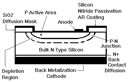
Silicon photodiodes are constructed from single crystal silicon wafers . The purity of silicon is directly related to its resistivity, with higher resistivity indicating higher purity silicon.  A cross section of a typical silicon photodiode is shown in the figure. N type silicon is the starting material. A thin "p" layer is formed on the front surface of the device by thermal diffusion or ion implantation of the appropriate doping material (usually boron). The interface between the "p" layer and the "n" silicon is known as a pn junction. Small metal contacts are applied to the front surface of the device and the entire back is coated with a contact metal. The back contact is the cathode, the front contact is the anode. The active area is coated with either silicon nitride, silicon monoxide or silicon dioxide for protection and to serve as an anti-reflection coating. The thickness of this coating is optimized for particular irradiation wavelengths. As an example, a Centro Vision Series 5-T photodiode has a coating which enhances its response to the blue part of the spectrum.


Photodiode junctions are unusual because the top "p" layer is very thin. The thickness of this layer is determined by the wavelength of radiation to be detected. Near the pn junction the silicon becomes depleted of electrical charges. This is known as the "depletion region". The depth of the depletion region can be varied by applying a reverse bias voltage across the junction. When the depletion region reaches the back of the diode the photodiode is said to be "fully depleted". The depletion region is important to photodiode performance since most of the sensitivity to radiation originates there. The capacitance of the pn junction depends on the thickness of this variable depletion region. Increasing the bias voltage increases the depth of this region and lowers capacitance until the fully depleted condition is achieved. Junction capacitance is also a function of the resistivity of silicon used and active area size.        


Due to concentration gradient, the diffusion of electrons from the N- type region to the P-type region and the diffusion of holes from the P- type region to the N-type region, develops a built-in voltage across
the junction. The inter-diffusion of electrons and holes between the N and P regions across the junction results in a region with no free carri- ers. This is the depletion region. The built-in voltage across the deple- tion region results in an electric field with maximum at the junction and no field outside of the depletion region. Any applied reverse bias adds to the built in voltage and results in a wider depletion region.The electron-hole pairs generated by light are swept away by drift inthe depletion region and are collected by diffusion from the undepleted region. The current generated is proportional to the incident light or radiation power. The light is absorbed exponentially with distance and is proportional to the absorption coefficient. The absorption coefficient is very high for shorter wavelengths in the UV region and is small for longer wavelengths . Hence, short wavelength photons such as UV, are absorbed in a thin top surface layer while silicon becomes transparent to light wavelengths longer than 1200 nm. Moreover, photons with energies smaller than the band gap are not absorbed at all. The boundaries of the depletion region act as the plates of a parallel plate capacitor. The junction capacitance is directly proportional to the diffused area and inversely proportional to the width of the depletion region. In addition, higher resistivity substrates have lower junction capacitance. In photoconductive mode (reverse biased), however, the drift current becomes the dominant current (dark current) and varies directly with temperature.
As time constant is directly proportional to capacitance, therefore, lower the capacitance, lesser will br time constant and hence lesser will be response time.

Tunnel Diode


In a conventional semiconductor diode, conduction takes place while the p–n junction is forward biased and blocks current flow when the junction is reverse biased. This occurs up to a point known as the “reverse breakdown voltage” when conduction begins (often accompanied by destruction of the device). In the tunnel diode, the dopant concentration in the p and n layers are increased to the point where the reverse breakdown voltage becomes zero and the diode conducts in the reverse direction.
This reverse resistance occurs because as doping is increased, reverse voltage will decrease and a time will come when there will be reverse  breakdown voltage in forward bias condition. The application of a reverse voltage to the p-n junction will cause a transient current to flow as both electrons and holes are pulled away from the junction. When the potential formed by the widened depletion layer equals the applied voltage, the current will cease except for the small thermal current i.e. as voltage will increase , current will  decrease.


However, when forward-biased, an odd effect occurs called “quantum mechanical tunnelling” which gives rise to a region where an increase in forward voltage is accompanied by a decrease in forward current due to change in conduction band position. Quantum tunnelling refers to the quantum mechanical phenomenon where a particle tunnels  i.e. transmitted through a barrier that it classically could not be able to cross.Barrier is the depletion region of p-n junction.


                                                              dynatron oscillator

This negative resistance region can be used  in  the dynatron oscillator .A dynatron oscillator is an electronic circuit that uses negative resistance to keep an LC tank circuit oscillating .If an ideal capacitor is connected in parallel with an ideal inductor, they form a resonant circuit that, once it begins oscillating, will oscillate forever as the energy is transferred back and forth between the capacitor and the inductor.In practice, however, the two components are not ideal. Real inductors and capacitors are equivalent to an ideal component in parallel (or in series) with a resistance; a real resonant circuit is equivalent to an ideal capacitor, inductor, and resistor connected in parallel. If a negative resistance equal in magnitude to this positive resistance can be connected in parallel with the above circuit, then the two resistances will cancel and the circuit will oscillate forever .